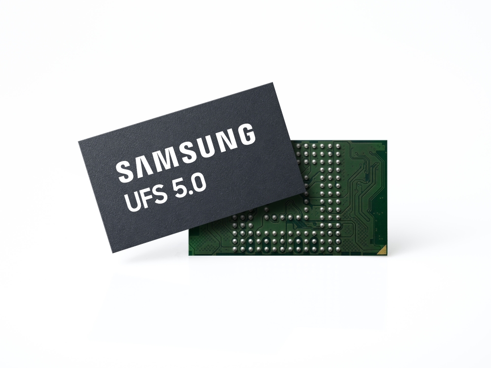
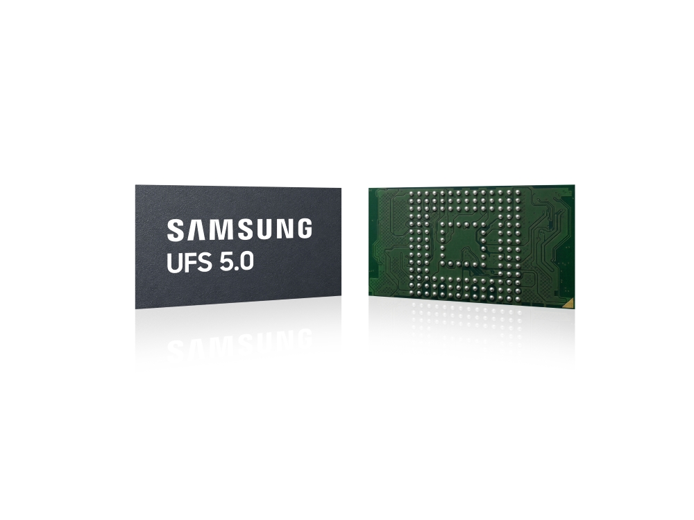
Samsung Unveils Industry’s Fastest UFS 5.0 Solution for Next-Gen On-Device AI Applications
Samsung Electronics, the world leader in advanced memory technology today announced that, for the first time in the industry, it has developed the industry’s fastest Universal Flash Storage (UFS) 5.0 solution, which will help enable seamless and highly efficient AI services on future mobile devices.
The milestone sets a new benchmark for the next-generation mobile memory market as the enhanced performance is expected to allow mobile device users with significantly reduced latency and faster response times when running large language models (LLMs) in on-device AI environments.
“In the era of on-device AI, storage devices are evolving into a key driver defining AI experiences,” said Jangseok Choi, head of Memory Product Planning at Samsung Electronics. “As we successfully move beyond the development stage of the industry’s first UFS 5.0 solution, Samsung is setting a new standard for storage on the go and will continue to drive innovation for the next-generation mobile platform market.”
Generative AI is rapidly shifting from the cloud to the device, driving a surge in the scale of data required for local processing. As a result, storage is evolving from a medium used primarily to store data to core infrastructure that supports AI computation.
Samsung’s UFS 5.0 integrates the latest embedded memory interface standard from JEDEC, achieving unparalleled performance levels with the industry’s highest bandwidth of up to 10.8 gigabytes per second (GB/s).
The new storage solution delivers a sequential read speed of up to 10.8 GB/s and a sequential write speed of up to 9.5 GB/s, speeds that are respectively more than twice as fast as those of the previous UFS 4.1 standard. This significant advancement enables much faster storage and processing of large data for on-device AI applications.
Power efficiency in Samsung’s UFS 5.0 is also improved by more than 40% compared to the company’s UFS 4.1 solution. This is achieved by implementing a number of new innovations, including clock gating and multi-voltage technologies. These enhancements help to considerably reduce the power required to transfer the same amount of data, drastically lowering overall power consumption and extending the battery life of next-generation mobile devices.
Samsung has engineered the UFS 5.0 solution into an ultra-compact package measuring just 7.5mm x 13mm x 0.9mm — making it 16.7% smaller than its predecessor. This form factor significantly boosts design flexibility and internal space utilization for a wide range of applications, including mobile, wearable and extended reality (XR) devices.
Samsung will begin mass production of its UFS 5.0 in the fourth quarter of this year in a variety of capacities up to one terabyte (TB). Through this breakthrough in UFS 5.0 technology, Samsung is staying ahead of industry needs and plans to scale up supply to meet the growth of next-generation device markets — ranging from flagship smartphones to XR headsets and AI wearables.
通知: 通过本系统在互联网上发布的任何文字内容,并不一定代表本网站或其作者的观点。通过本系统发布的评论,其全部责任及作者身份均由使用该系统的读者独自承担。本网站管理方保留自行决定删除其认为具有冒犯性、诽谤性、中伤性、带有偏见或以任何方式对第三方造成伤害的评论及文字内容的权利。具有宣传性质或未提供作者真实身份信息(全名及有效电子邮箱地址)的文本也可能被删除。